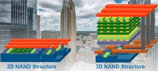
For logic products, the process development emphasis would be on increasing the number of metal levels and their connections to vertical transistors. For DRAM products, the emphasis would be on adding memory cells that are located in layers vertically above the silicon substrate surface.
The article from semiengineering.com accessed via the link below discusses processing issues such as, “the challenges here are focused on variability control of several key processes…. Alternating stack deposition must have precise control with good uniformities and low defectivity. Initially, the uniformities must be good,” Applied’s Ping said. “It’s all going back to stress control because the alternating films are different. For each film, there could be a mismatch. Stress could show up.” “Repeatability at every single step is also critical, and it has to be done at high productivity in order to keep costs down,” “Tiny trenches or channels are etched from the top of the device to the substrate. To illustrate the complexity of this step, Samsung’s 3D NAND device has 2.5 million tiny channels in the same chip. Each of them must be parallel and uniform.” One area that the article does not mention is the additional circuitry complication of the 3D NAND products. For example, there is a need to sense correctly and repeatedly every one of the larger number of smaller memory cells that are on each 3D NAND. Also, the controller of the 3D NAND has to deal with the larger number of memory cells that need to be accessed and controlled. How to Make 3D NAND
1 Comment
|
AuthorRon Maltiel, Archives
November 2017
Categories
All
|
 RSS Feed
|
RMG & Associates, Inc.
(408) 446-3040 Saratoga, CA 95080 |
|
|
© 2024 RMG & Associates, Inc.