Interconnect Issues: History and Future Prospects, Part 2
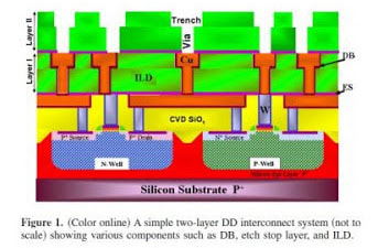
Ahmet Ceyhan and Azad Naeemi, Georgia Institute of Technology Paper synopsis below. The research pipeline of the semiconductor industry involves increasingly radical potential solutions to carry technology advancement through dimensional scaling to beyond-conventional CMOS. Many logic devices are under investigation to extend Moore’s Law to beyond the year 2020. These logic devices differ in structure and operating principles, and include various physical quantities that may be used for encoding information, such as charge, electric dipole, magnetic dipole (spin), orbital state, mechanical position, light intensity, etc. However, any device technology that offers advantages in performance, power dissipation or ease in dimensional scaling will have to be complemented with an interconnect technology that offers similar trades to avoid major bottlenecks due to interconnects. Various carbon-based interconnects were shown to have comparable or better performance compared to Cu/low-k in terms of both resistance-capacitance (RC) product and energy-delay-product (EDP). The aim of this article is to investigate the interactions of interconnects with various voltage-controlled, charge-based devices similar to the conventional Si-CMOS transistor, including high-performance and ultra-low-power options. For that purpose, we pair finFETs, MOSFET-like carbon nanotube FETs (CNFETs), homojunction III-V tunnel FETs (TFETs) and sub-threshold CMOS devices with conventional Cu/low-k and emerging interconnect options; and we compare the relative performances at the circuit level. These device and interconnect technology options are illustrated in Figure 1. Since various device technologies offer very different characteristics in terms of the output current, input capacitance, subthreshold swing, etc., the constraints that they put on interconnects and the best interconnect option for each device are different as well. This difference stems from the fact that the impacts of technology parameters of various interconnect technologies on the speed and energy advantages of a circuit may differ depending on the transistors used. Emerging carbon nanotube (CNT) and graphene nanoribbon (GNR) interconnects are mostly more resistive than Cu/low-k [3,4], but they offer lower capacitances. Based on the Berkeley Short-channel IGFET Common Gate Model (BSIM-CMG),[5] predictive technology models (PTMs) for finFET devices are developed jointly by the Arizona State University PTM Group and ARM.[6] The development of the model parameters for the BSIM-CMG model is performed using the scaling theory of multi-gate devices, physical models and ITRS projections. Compared to planar bulk CMOS devices, finFET devices have significantly improved short channel effects (SCE) due to better electrostatics, can carry more current and offer improved area efficiency. The channel width is quantized; hence, the number of fins has to be optimized for drive current choices. CNFET devices are alternative solutions to performance enhancement of transistors in the “atomic dimension limit” beyond 2020. A compact model developed by Deng et al.[7] is calibrated to meet reasonable ON current requirements while controlling the threshold voltage to keep leakage current at a reasonable value; and used for simulating MOSFET-like CNFET gates at the 16 nm technology node to predict the circuit- and system-level properties of CNFET devices. This model includes various non-idealities, such as the quantum confinement effects on both circumferential and axial directions, elastic scattering in the channel region, the resistive source/drain, the Schottky-barrier resistance, the acoustical and phonon scattering in the channel region, the screening effect by the parallel CNTs in CNFETs that contain multiple parallel CNTs under the same gate, and parasitic gate capacitances.
1 Comment
5/8/2024 03:17:22 pm
Interesting thoughts, I really enjoyed your blog. Leave a Reply. |
AuthorRon Maltiel, Archives
November 2017
Categories
All
|
 RSS Feed
|
RMG & Associates, Inc.
(408) 446-3040 Saratoga, CA 95080 |
|
|
© 2024 RMG & Associates, Inc.