RMG & Associates
  • Services
    • Circuit Consulting
    • Process Consulting
    • Manufacturing Consulting
  • Semiconductor Process
    • Semiconductor Process News
    • Products & Devices Technology
    • Educational Information
    • Industry Glossary
    • ITRS Documents
    • Technical Database
  • Semiconductor Circuits
    • Semiconductor Circuit News
    • Education & Classes
    • Circuit Glossary & Data Sheets
  • Flash Memory
    • Flash Memory News
    • Products & Devices
    • Flash Memory Education
    • Flash Memory Resource Links
  • Patents
    • Patent News
    • Patent Resources
    • RMG Patents
  • Blog
  • About
  • Contact

Semiconductor Expert Blog

Industry mergers / circuits / process / flash memory / manufacturing

Process Challenges of 3D (Vertical Transistors)

6/9/2016

0 Comments

 
Picture

​The article linked in this blog describes the drive toward 3D vertical transistors above the surface of the chip's die. 3D NAND represents a major departure from today’s planar NAND. 
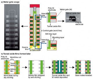
.In 2D NAND, the fabrication process is dependent on advanced lithography. In 3D NAND, though, vendors are using trailing-edge 40 nm to 20 nm design rules. Lithography is still used, but it isn’t the most critical step. So for 3D NAND, the challenges shift from lithography to deposition and etch.

However, the new 3D processes are not easy to implement.

3D NAND introduces a number of new and difficult process steps to the semiconductor industry…it has introduced several fairly complex and new processes. Uniformity of these processes is critical. So, from my perspective, the challenges here are focused on variability control of several key processes.

It will be interesting how well Intel and Micron XPoint (see
 SSD, 3D Vertical NAND, or 3D XPoint?) products will succeed against current 3D products (see November 2012 3D NAND flash is coming).

​Read more in the semiengineering.com article: How to Make 3D NAND.
0 Comments


Leave a Reply.

    Author

    Ron Maltiel,
    RMG & Associates Principal

    Archives

    November 2017
    November 2016
    September 2016
    July 2016
    June 2016
    May 2016
    April 2016
    March 2016
    July 2013

    Categories

    All
    3D Manufacturing
    3D NAND
    3D Vertical NAND
    Analog Devices
    ARM
    Bill Of Materials
    Broacdcom
    Brocade
    Cavium
    Chips
    DRAM
    Fabrication
    Flash
    Flash Memory News
    Foundries
    Interconnect
    IoT
    IPhone
    IPhone 7
    IPhone SE
    Linear
    Manufacturing
    Micron
    Microsemi
    NAND
    QLogic
    Samsung
    SDRAM
    Semiconductor Acquisitions
    Semiconductor Industry News
    Semiconductor Mergers
    Semiconductor Process News
    Semi.org
    Skyworks
    Softbank
    SSD
    Teardown
    TSMC
    XPoint

    RSS Feed

Picture
RMG & Associates, Inc.
(408) 446-3040
​Saratoga, CA 95080
SERVICES
Process Consulting

Circuits Consulting
Manufacturing Consulting
SEMICONDUCTOR PROCESS
Semiconductor Process 
Products & Devices
Educational Information
Industry Glossary
Process Technical Reference
Technical Database
SEMICONDUCTOR CIRCUITS
Semiconductor Circuit News
Education & Classes
Industry Glossary & Data Sheets
FLASH MEMORY
Non-Volatile Flash Memory News
Products & Devices
Flash Education
Resources & Links
PATENTS
Patent News
Patent Resources
Ron Maltiel Patents
BLOG
ABOUT
CONTACT US
© 2024 RMG & Associates, Inc. 
  • Services
    • Circuit Consulting
    • Process Consulting
    • Manufacturing Consulting
  • Semiconductor Process
    • Semiconductor Process News
    • Products & Devices Technology
    • Educational Information
    • Industry Glossary
    • ITRS Documents
    • Technical Database
  • Semiconductor Circuits
    • Semiconductor Circuit News
    • Education & Classes
    • Circuit Glossary & Data Sheets
  • Flash Memory
    • Flash Memory News
    • Products & Devices
    • Flash Memory Education
    • Flash Memory Resource Links
  • Patents
    • Patent News
    • Patent Resources
    • RMG Patents
  • Blog
  • About
  • Contact